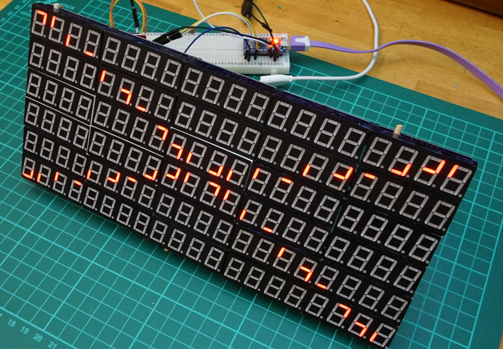
Or an 840 Segment display (960 if you count the decimal point)
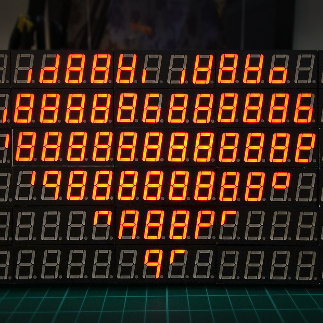
What’s going on here then?
It all started with an eBay purchase of some cheap Chinese 7 segment displays.
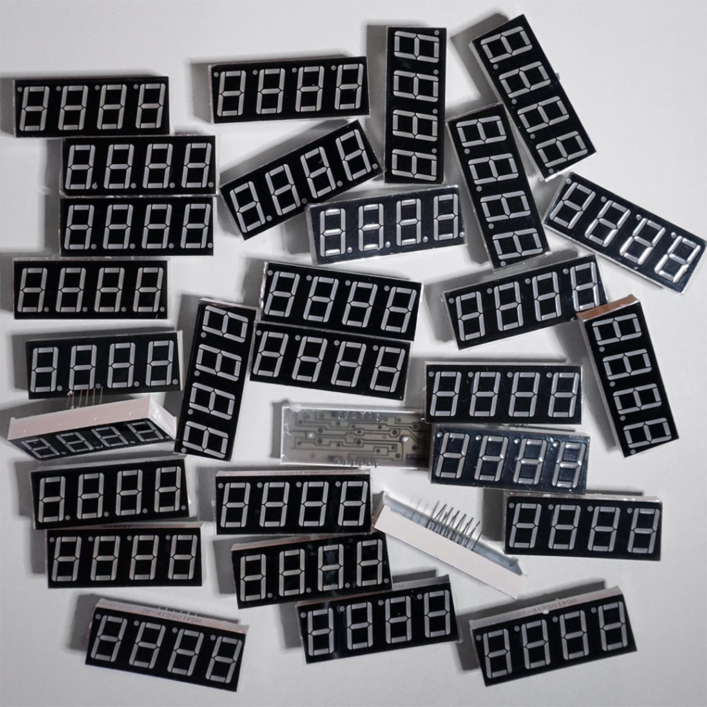
A month or two later and bag of 30 arrived! Did I really buy 30? I soon realised that these 7 segment displays were common anode and wouldn’t work nicely with my old friend the Max7219. I eventually figured out a bodge [common anode displays on the Max7219 and an Arduino] and, another eBay purchase later, I had a bag full of Max7219s too.
I then designed a PCB to drive 2 of these 4 digit packages. That’s 64 LEDs, the total number a single Max7219 can drive. The PCB needed to be smaller than the 2 displays if I wanted to stick these modules together into one big array.
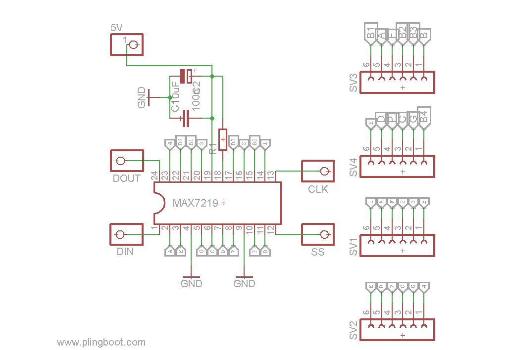 Circuit diagram : Max7219 driving 2 common anode 4×7 segment displays
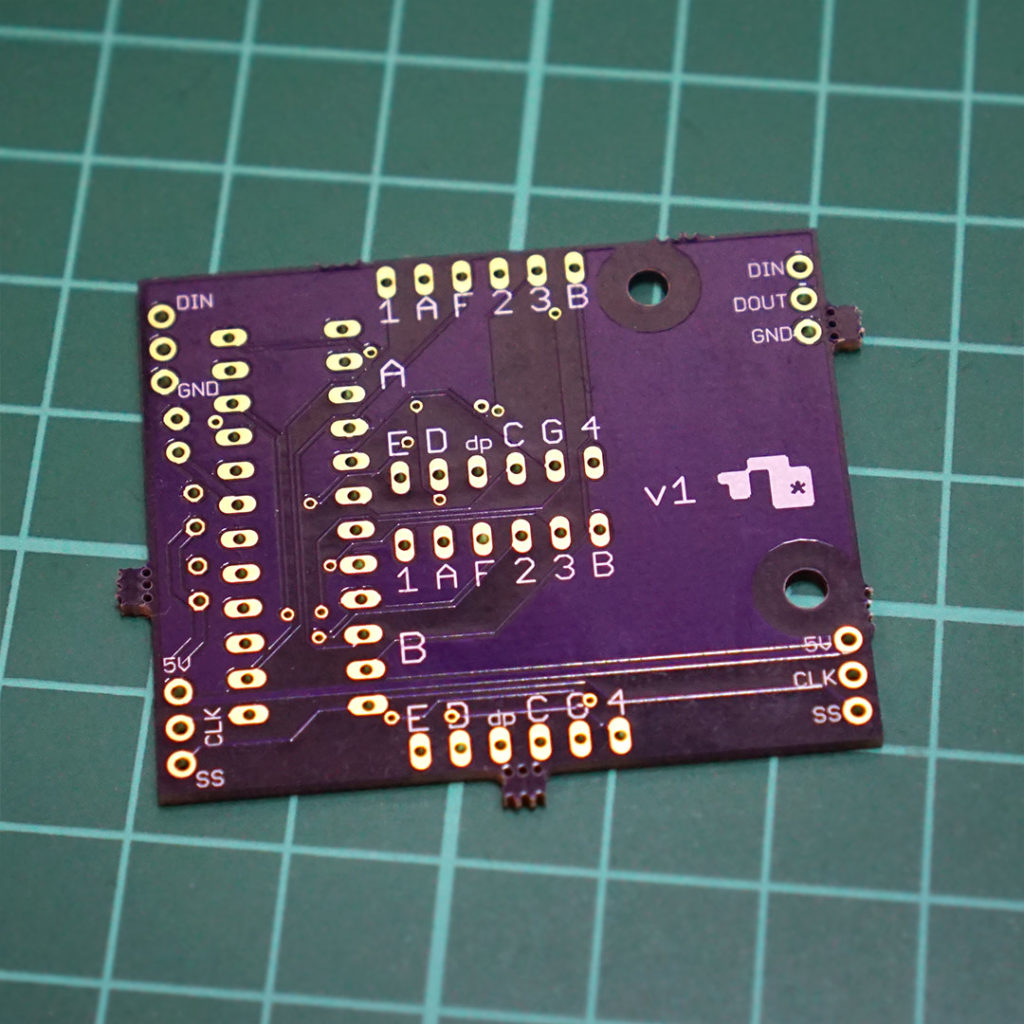 Finished PCB
Daisy chaining multiple Max7219s
One of the great things about the Max7219 is that they can be chained together. Data Out (pin 24) carries across to the Data In (pin 1) of another max7219 and so on. Doing this means I can control many more than 64 LEDs. I designed the PCB with this in mind with the idea that they would be nice and modular, slotting together effortlessly. It didn’t quite work and was misaligned. Nothing a soldering iron and some wire couldn’t fix.
I’d never coded for multiple Max7219s before and strangely couldn’t find much online.
A standard function to send data to a Max7219 would look something like this :
void MAX7219Send(uint8_t address, uint8_t value)
{
  // Ensure LOAD/CS is LOW
  digitalWrite(chip_select, LOW);

  // Send the register address
  SPI.transfer(address);

  // Send the value
  SPI.transfer(value);

  // Tell chip to load in data
  digitalWrite(chip_select, HIGH);
}
After some experimenting I discovered it was pretty easy to address multiple Max7219s from my Arduino Pro Micro clone. To write to three would look something like :
void MAX7219Send(uint8_t address_A, uint8_t value_A, uint8_t address_B, uint8_t value_B, uint8_t address_C, uint8_t value_C)
{
  // Ensure LOAD/CS is LOW
  digitalWrite(chip_select, LOW);

  // Send the register address
  SPI.transfer(address_A);

  // Send the value
  SPI.transfer(value_A);

  // Send the register address
  SPI.transfer(address_B);

  // Send the value
  SPI.transfer(value_B);

  // Send the register address
  SPI.transfer(address_C);

  // Send the value
  SPI.transfer(value_C);

  // Tell chip to load in data
  digitalWrite(chip_select, HIGH);
}
At this point, I’ve got a few connected together and I’m beginning to think about how I’m going to display bitmaps, or single ‘pixels’, on this thing.
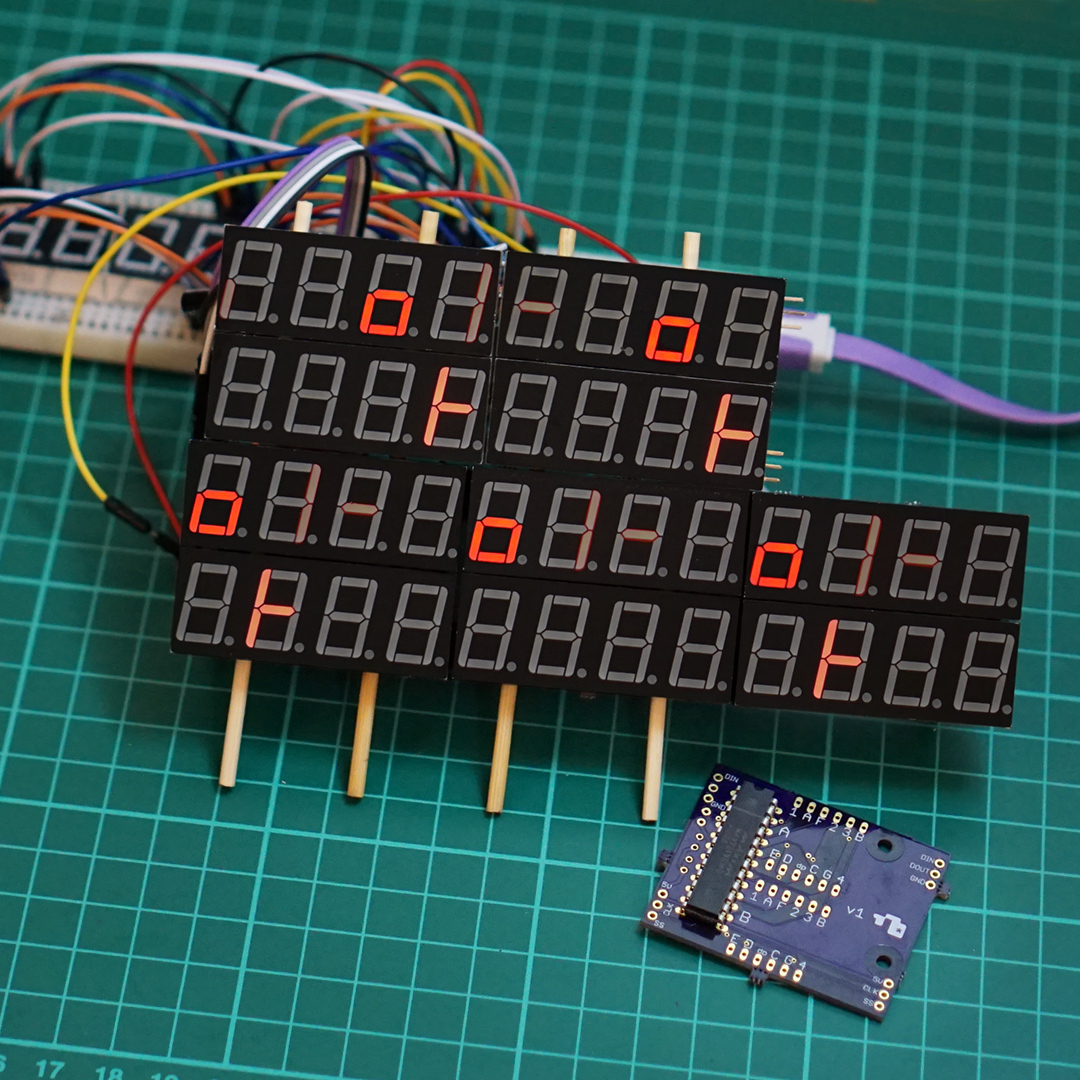 Held together with wooden skewers
Mapping pixels to segments
I ordered more PCBs, this 7 segment folly was becoming pretty expensive. In total I’d have a bank of 5 x 3 modules, that’s 20 x 6 digits. If each 7 segment digit corresponds to a 2 x 4 pixel block then that would give me a virtual screen size of 40 x 30 pixels. A single 8 digit module would map to a 8 x 10 pixel area, like this :
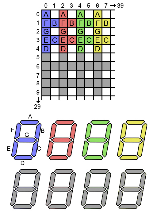 Pixel buffer mapping to segments
Notice there’s a lot of pixels here that don’t map to any segments, 30% that will never be displayed.
I created a 40 x 30 1 bpp screen buffer and will use standard routines to put pixels, draw lines, copy bitmaps etc. into this buffer before, somehow, translating that lot to the 7 segment displays.
The data structure for my screen buffer looks like :
byte screen_buffer[30][5] =
{
  //   bank 0       bank 1       bank 2        bank 3        bank 4
  // top
  { 0b00000000,   0b00000000,   0b00000000,   0b00000000,   0b00000000,},
  { 0b00000000,   0b00000000,   0b00000000,   0b00000000,   0b00000000,},
  { 0b00000000,   0b00000000,   0b00000000,   0b00000000,   0b00000000,},
  { 0b00000000,   0b00000000,   0b00000000,   0b00000000,   0b00000000,},
  { 0b00000000,   0b00000000,   0b00000000,   0b00000000,   0b00000000,},
  // lower
  { 0b00000000,   0b00000000,   0b00000000,   0b00000000,   0b00000000,},
  { 0b00000000,   0b00000000,   0b00000000,   0b00000000,   0b00000000,},
  { 0b00000000,   0b00000000,   0b00000000,   0b00000000,   0b00000000,},
  { 0b00000000,   0b00000000,   0b00000000,   0b00000000,   0b00000000,},
  { 0b00000000,   0b00000000,   0b00000000,   0b00000000,   0b00000000,},
  //   bank 0       bank 1       bank 2        bank 3        bank 4
  // top
  { 0b00000000,   0b00000000,   0b00000000,   0b00000000,   0b00000000,},
  { 0b00000000,   0b00000000,   0b00000000,   0b00000000,   0b00000000,},
  { 0b00000000,   0b00000000,   0b00000000,   0b00000000,   0b00000000,},
  { 0b00000000,   0b00000000,   0b00000000,   0b00000000,   0b00000000,},
  { 0b00000000,   0b00000000,   0b00000000,   0b00000000,   0b00000000,},
  // lower
  { 0b00000000,   0b00000000,   0b00000000,   0b00000000,   0b00000000,},
  { 0b00000000,   0b00000000,   0b00000000,   0b00000000,   0b00000000,},
  { 0b00000000,   0b00000000,   0b00000000,   0b00000000,   0b00000000,},
  { 0b00000000,   0b00000000,   0b00000000,   0b00000000,   0b00000000,},
  { 0b00000000,   0b00000000,   0b00000000,   0b00000000,   0b00000000,}
};
Standard putPixel(x,y) and removePixel(x,y) routines are pretty straightforward, just a matter of turning bits on and off in the screen buffer :
void removePixel(byte x, byte y)
{
  byte bank = x / 8;
  byte by = y;
  byte thebit = 0b10000000 >> ((x % 8)); // bit to turn off
  screen_buffer[by][bank] &= ~thebit;
}

void putPixel(byte x, byte y)
{
  byte bank = x / 8;
  byte by = y;
  byte thebyte = 0b10000000 >> ((x % 8));
  screen_buffer[by][bank] |= thebyte;
}
Displaying the screen buffer on the 7 segment array is a little more complicated, partly because the Max7219s are wired in reverse (the common anode problem). This made my code slightly more weird than it would've been if I was using common cathode displays.
In short, the usual digit parameter of a Max7219 command now refers to the segment and the data refers to the digit, or any number of the 8 addressable digits.
Normally, to set the C segment on digit 1 you would use the command :
MAX7219Send(1,0b00010000);
But with my reversed, common anode, wiring to set the C segment on digit 1 it's :
MAX7219Send(3,0b00000001);
Or to set the C segment on all digits :
MAX7219Send(3,0b01111111);
My idea then, to loop through 7 segments and build the bit pattern to send for each digit of a module / bank, for each of the 15 modules.
Given the digit (0 to 7) and the bank(0 to 14) I have to grab and convert the pixel data from the screen buffer for each digit and bank I'm looking at.
Anyway, here's the confusing code :
// returns current screen buffer segment bit state for given bank and digit
byte get_screen_buffer(byte digit, byte bank)
{
  // x,y into screen buffer from digit, bank
  byte bx = (bank % 5);
  byte by = ((digit / 4) ) * 5 + ((bank / 5) * 10);

  byte segs = 0;
  byte shift = 6 - 2 * (digit % 4);

  bool bittest;
 /*
   pixel to digit mapping :
   A,x,
   F,B,
   G,x,
   E,C,
   D,x

   0,0 = A
   0,1 = F
   1,1 = B
   0,2 = G
   0,3 = E
   1,3 = C
   0,4 = D
   */

  //A
  bittest =  ( ( (screen_buffer[by][bx]) & (0b00000010 << shift )  ) >> shift );
  segs  = segs | ( (bittest * 255) & 0b1000000);
  //B
  bittest =  ( ( (screen_buffer[by + 1][bx]) & (0b00000001 << shift )  ) >> shift );
  segs  = segs | ((bittest * 255) & 0b0100000);
  //C
  bittest =  ( ( (screen_buffer[by + 3][bx]) & (0b00000001 << shift )  ) >> shift );
  segs  = segs | ((bittest * 255) & 0b0010000);
  //D
  bittest =  ( ( (screen_buffer[by + 4][bx]) & (0b00000010 << shift )  ) >> shift );
  segs  = segs | ((bittest * 255) & 0b0001000);
  //E
  bittest =  ( ( (screen_buffer[by + 3][bx]) & (0b00000010 << shift )  ) >> shift );
  segs  = segs | ((bittest * 255) & 0b0000100);
  //F
  bittest =  ( ( (screen_buffer[by + 1][bx]) & (0b00000010 << shift )  ) >> shift );
  segs  = segs | ((bittest * 255) & 0b0000010);
  //G
  bittest =  ( ( (screen_buffer[by + 2][bx]) & (0b00000010 << shift )  ) >> shift );
  segs  = segs | ((bittest * 255) & 0b0000001);

  return segs;
}


#define DIGIT1 0b01000000
#define DIGIT2 0b00100000
#define DIGIT3 0b00010000
#define DIGIT4 0b00001000

#define DIGIT5 0b00000100
#define DIGIT6 0b00000010
#define DIGIT7 0b00000001
#define DIGIT8 0b10000000

byte display_digits[]
{
  DIGIT1,
  DIGIT2,
  DIGIT3,
  DIGIT4,

  DIGIT5,
  DIGIT6,
  DIGIT7,
  DIGIT8
};

byte bank[15];

byte segment_lookup[] =
{
   0b1000000, //A
   0b0100000, //B
   0b0010000, //C
   0b0001000, //D
   0b0000100, //E
   0b0000010, //F
   0b0000001  //G
};

void display_screen_buffer()
{
// Each max7219 controls 1 bank of 8 digits.
// for each 7-seg segment (A to F) of a digit
  for (byte segments = 0; segments < 7; segments++)
  {
      // clear
      for(byte bank_i=0;bank_i<15;bank_i++) bank[bank_i] = 0b00000000;

      // with each segment, loop through 8 digits of a bank
      for (byte d = 0; d < 8; d++)
      {
         //15 banks
         for(byte bank_i=0;bank_i<15;bank_i++)
         {
             // work out which segments we're addressing at this bank
             byte segtosend = get_screen_buffer(d, bank_i) & segment_lookup[segments] ;
             if (segtosend) bank[bank_i] =  (bank[bank_i] | display_digits[d]);
         }
      }
      MAX7219Send(
      segments + 1, bank[4], segments + 1, bank[3], segments + 1, bank[2], segments + 1, bank[1], segments + 1, bank[0],
      segments + 1, bank[9], segments + 1, bank[8], segments + 1, bank[7], segments + 1, bank[6], segments + 1, bank[5],
      segments + 1, bank[14], segments + 1, bank[13], segments + 1, bank[12], segments + 1, bank[11], segments + 1, bank[10]);
   }
}
It works! No doubt this could all be optimised, a lot. An obvious optimise would be to simply replace those common anode displays with ones that play nicely with the MAX7219 and remove the need for all this crazy reverse wiring and weird addressing, although it'd probably only be slightly less confusing.

Anyway here's the, slightly more complete, full code :
#include
#define LOAD_PIN 10

byte screen_buffer[30][5] =
{
  //   bank 0       bank 1       bank 2     bank 3        bank 4
  // top
  { 0b00000000,   0b00000000,   0b00000000, 0b00000000,   0b00000000,},
  { 0b00000000,   0b00000000,   0b00000000, 0b00000000,   0b00000000,},
  { 0b00000000,   0b00000000,   0b00000000, 0b00000000,   0b00000000,},
  { 0b00000000,   0b00000000,   0b00000000, 0b00000000,   0b00000000,},
  { 0b00000000,   0b00000000,   0b00000000, 0b00000000,   0b00000000,},
  // lower
  { 0b00000000,   0b00000000,   0b00000000, 0b00000000,   0b00000000,},
  { 0b00000000,   0b00000000,   0b00000000, 0b00000000,   0b00000000,},
  { 0b00000000,   0b00000000,   0b00000000, 0b00000000,   0b00000000,},
  { 0b00000000,   0b00000000,   0b00000000, 0b00000000,   0b00000000,},
  { 0b00000000,   0b00000000,   0b00000000, 0b00000000,   0b00000000,},
  //   bank 0       bank 1       bank 2     bank 3        bank 4
  // top
  { 0b00000000,   0b00000000,   0b00000000, 0b00000000,   0b00000000,},
  { 0b00000000,   0b00000000,   0b00000000, 0b00000000,   0b00000000,},
  { 0b00000000,   0b00000000,   0b00000000, 0b00000000,   0b00000000,},
  { 0b00000000,   0b00000000,   0b00000000, 0b00000000,   0b00000000,},
  { 0b00000000,   0b00000000,   0b00000000, 0b00000000,   0b00000000,},
  // lower
  { 0b00000000,   0b00000000,   0b00000000, 0b00000000,   0b00000000,},
  { 0b00000000,   0b00000000,   0b00000000, 0b00000000,   0b00000000,},
  { 0b00000000,   0b00000000,   0b00000000, 0b00000000,   0b00000000,},
  { 0b00000000,   0b00000000,   0b00000000, 0b00000000,   0b00000000,},
  { 0b00000000,   0b00000000,   0b00000000, 0b00000000,   0b00000000,}

};


// returns current screen buffer segment bit state for given bank and digit
byte get_screen_buffer(byte digit, byte bank)
{
  // x,y into screen buffer from digit, bank
  byte bx = (bank % 5);
  byte by = ((digit / 4) ) * 5 + ((bank / 5) * 10);

  byte segs = 0;
/*
  byte shift;
  if (digit == 0) shift = 6;
  if (digit == 1) shift = 4;
  if (digit == 2) shift = 2;
  if (digit == 3) shift = 0;

  if (digit == 4) shift = 6;
  if (digit == 5) shift = 4;
  if (digit == 6) shift = 2;
  if (digit == 7) shift = 0;
*/
  byte shift = 6 - 2 * (digit % 4);
  bool bittest;
 /*
   pixel to digit mapping :
   A,x,
   F,B,
   G,x,
   E,C,
   D,x

   0,0 = A
   0,1 = F
   1,1 = B
   0,2 = G
   0,3 = E
   1,3 = C
   0,4 = D

   */

  //A
  bittest =  ( ( (screen_buffer[by][bx]) & (0b00000010 << shift )  ) >> shift );
  segs  = segs | ( (bittest * 255) & 0b1000000);
  //B
  bittest =  ( ( (screen_buffer[by + 1][bx]) & (0b00000001 << shift )  ) >> shift );
  segs  = segs | ((bittest * 255) & 0b0100000);
  //C
  bittest =  ( ( (screen_buffer[by + 3][bx]) & (0b00000001 << shift )  ) >> shift );
  segs  = segs | ((bittest * 255) & 0b0010000);
  //D
  bittest =  ( ( (screen_buffer[by + 4][bx]) & (0b00000010 << shift )  ) >> shift );
  segs  = segs | ((bittest * 255) & 0b0001000);
  //E
  bittest =  ( ( (screen_buffer[by + 3][bx]) & (0b00000010 << shift )  ) >> shift );
  segs  = segs | ((bittest * 255) & 0b0000100);
  //F
  bittest =  ( ( (screen_buffer[by + 1][bx]) & (0b00000010 << shift )  ) >> shift );
  segs  = segs | ((bittest * 255) & 0b0000010);
  //G
  bittest =  ( ( (screen_buffer[by + 2][bx]) & (0b00000010 << shift )  ) >> shift );
  segs  = segs | ((bittest * 255) & 0b0000001);

  return segs;
}

void putpixel(byte x, byte y)
{
// bounds check
if ((x>=0) && (x<40) &&(y>=0) && (y<30))
{
  // which bank
  byte bank = x / 8;
  byte by = y;
  //byte thebyte = 1 << (8-(x % 8));
  byte thebyte = 0b10000000 >> ((x % 8));

  screen_buffer[by][bank] |= thebyte;
}
}

bool getpixel(byte x, byte y, bool setclear)
{
  // which bank
  byte bank = x / 8;
  byte by = y;
  byte thebit = 0b10000000 >> ((x % 8));

  byte check = screen_buffer[by][bank] & thebit;

  bool result = check << ((x % 8));

  return  result;

}

void removepixel(byte x, byte y)
{
  byte bank = x / 8;
  byte by = y;
  byte thebit = 0b10000000 >> ((x % 8)); // bit to turn off

  screen_buffer[by][bank] &= ~thebit;
}

#define DIGIT1 0b01000000
#define DIGIT2 0b00100000
#define DIGIT3 0b00010000
#define DIGIT4 0b00001000

#define DIGIT5 0b00000100
#define DIGIT6 0b00000010
#define DIGIT7 0b00000001
#define DIGIT8 0b10000000

byte display_digits[]
{
  DIGIT1,
  DIGIT2,
  DIGIT3,
  DIGIT4,

  DIGIT5,
  DIGIT6,
  DIGIT7,
  DIGIT8
};

byte bank[15];

byte segment_lookup[] =
{
  0b1000000, //A
  0b0100000, //B
  0b0010000, //C
  0b0001000, //D
  0b0000100, //E
  0b0000010, //F
  0b0000001  //G
};

void display_screen_buffer()
{
// Each max7219 controls 1 bank of 8 digits.
// for each 7-seg segment (A to F) of a digit
  for (byte segments = 0; segments < 7; segments++)
  {
      // clear
      for(byte bank_i=0;bank_i<15;bank_i++) bank[bank_i] = 0b00000000;

      // with each segment, loop through 8 digits of a bank
      for (byte d = 0; d < 8; d++)
      {
         // bank 1 to 15
         for(byte bank_i=0;bank_i<15;bank_i++)
         {
             // work out which segments we're addressing at this bank
             byte segtosend = get_screen_buffer(d, bank_i) & segment_lookup[segments] ;
             if (segtosend) bank[bank_i] =  (bank[bank_i] | display_digits[d]);
         }
      }

      MAX7219Send(
      segments + 1, bank[4], segments + 1, bank[3], segments + 1, bank[2], segments + 1, bank[1], segments + 1, bank[0],
      segments + 1, bank[9], segments + 1, bank[8], segments + 1, bank[7], segments + 1, bank[6], segments + 1, bank[5],
      segments + 1, bank[14], segments + 1, bank[13], segments + 1, bank[12], segments + 1, bank[11], segments + 1, bank[10]);
   }
}

//Transfers data to a MAX7219 register.
// address : the register to load data into
// value : the data to store
void MAX7219Send(
  uint8_t address, uint8_t value,
  uint8_t addressb, uint8_t valueb,
  uint8_t addressc, uint8_t valuec,
  uint8_t addressd, uint8_t valued,
  uint8_t addresse, uint8_t valuee,
  uint8_t addressf, uint8_t valuef,
  uint8_t addressg, uint8_t valueg,
  uint8_t addressh, uint8_t valueh,
  uint8_t addressi, uint8_t valuei,
  uint8_t addressj, uint8_t valuej,
  uint8_t addressk, uint8_t valuek,
  uint8_t addressl, uint8_t valuel,
  uint8_t addressm, uint8_t valuem,
  uint8_t addressn, uint8_t valuen,
  uint8_t addresso, uint8_t valueo
) {
  // Ensure LOAD/CS is LOW
  digitalWrite(LOAD_PIN, LOW);

  SPI.transfer(0x00);
  SPI.transfer(0x00);

  // Send the register address
  SPI.transfer(address);
  // Send the value
  SPI.transfer(value);

  SPI.transfer(addressb);
  // Send the value
  SPI.transfer(valueb);


  SPI.transfer(addressc);
  // Send the value
  SPI.transfer(valuec);

  SPI.transfer(addressd);
  // Send the value
  SPI.transfer(valued);

  SPI.transfer(addresse);
  // Send the value
  SPI.transfer(valuee);

  SPI.transfer(addressf);
  // Send the value
  SPI.transfer(valuef);

  SPI.transfer(addressg);
  // Send the value
  SPI.transfer(valueg);

  SPI.transfer(addressh);
  // Send the value
  SPI.transfer(valueh);

  SPI.transfer(addressi);
  // Send the value
  SPI.transfer(valuei);

  SPI.transfer(addressj);
  // Send the value
  SPI.transfer(valuej);

  SPI.transfer(addressk);
  // Send the value
  SPI.transfer(valuek);

  SPI.transfer(addressl);
  // Send the value
  SPI.transfer(valuel);

  SPI.transfer(addressm);
  // Send the value
  SPI.transfer(valuem);

  SPI.transfer(addressn);
  // Send the value
  SPI.transfer(valuen);

  SPI.transfer(addresso);
  // Send the value
  SPI.transfer(valueo);

  // Tell chip to load in data
  digitalWrite(LOAD_PIN, HIGH);
}

void setup()
{
  // Set load pin to output
  pinMode(LOAD_PIN, OUTPUT);

  // Reverse the SPI transfer to send the MSB first
  SPI.setBitOrder(MSBFIRST);

  // Start SPI
  SPI.begin();

  // Initialise the Max7219
  MAX7219Send(
    0x0F, 0x01, 0x0F, 0x01, 0x0F, 0x01, 0x0F, 0x01, 0x0F, 0x01,
    0x0F, 0x01, 0x0F, 0x01, 0x0F, 0x01, 0x0F, 0x01, 0x0F, 0x01,
    0x0F, 0x01, 0x0F, 0x01, 0x0F, 0x01, 0x0F, 0x01, 0x0F, 0x01);

  MAX7219Send(
    0x0F, 0x00, 0x0F, 0x00, 0x0F, 0x00, 0x0F, 0x00, 0x0F, 0x00,
    0x0F, 0x00, 0x0F, 0x00, 0x0F, 0x00, 0x0F, 0x00, 0x0F, 0x00,
    0x0F, 0x00, 0x0F, 0x00, 0x0F, 0x00, 0x0F, 0x00, 0x0F, 0x00 );

  // Turn BCD mode off
  MAX7219Send(
    0x09, 0x00, 0x09, 0x00, 0x09, 0x00, 0x09, 0x00, 0x09, 0x00,
    0x09, 0x00, 0x09, 0x00, 0x09, 0x00, 0x09, 0x00, 0x09, 0x00,
    0x09, 0x00, 0x09, 0x00, 0x09, 0x00, 0x09, 0x00, 0x09, 0x00 );

  // Set intensity
  MAX7219Send(
    0x0A, 0x13, 0x0A, 0x13, 0x0A, 0x13, 0x0A, 0x13, 0x0A, 0x13,
    0x0A, 0x13, 0x0A, 0x13, 0x0A, 0x13, 0x0A, 0x13, 0x0A, 0x13,
    0x0A, 0x13, 0x0A, 0x13, 0x0A, 0x13, 0x0A, 0x13, 0x0A, 0x13
  );

  // Scan count
  MAX7219Send(
    0x0B, 0x07, 0x0B, 0x07, 0x0B, 0x07, 0x0B, 0x07, 0x0B, 0x07,
    0x0B, 0x07, 0x0B, 0x07, 0x0B, 0x07, 0x0B, 0x07, 0x0B, 0x07,
    0x0B, 0x07, 0x0B, 0x07, 0x0B, 0x07, 0x0B, 0x07, 0x0B, 0x07
  );

  // Turn on chip
  MAX7219Send(
    0x0C, 0x01, 0x0C, 0x01, 0x0C, 0x01, 0x0C, 0x01, 0x0C, 0x01,
    0x0C, 0x01, 0x0C, 0x01, 0x0C, 0x01, 0x0C, 0x01, 0x0C, 0x01,
    0x0C, 0x01, 0x0C, 0x01, 0x0C, 0x01, 0x0C, 0x01, 0x0C, 0x01
  );


 //clear all segments
 for (byte i =0;i<=8;i++)
 {
    MAX7219Send(
    i, 0x00, i, 0x00, i, 0x00, i, 0x00, i, 0x00,
    i, 0x00, i, 0x00, i, 0x00, i, 0x00, i, 0x00,
    i, 0x00, i, 0x00, i, 0x00, i, 0x00, i, 0x00);
 }

}


void drawLine( byte x1, byte y1, byte x2, byte y2)
{
  int tmp;
  int x,y;
  int dx, dy;
  int err;
  int ystep;

  int swapxy = 0;

  if ( x1 > x2 ) dx = x1-x2; else dx = x2-x1;
  if ( y1 > y2 ) dy = y1-y2; else dy = y2-y1;

  if ( dy > dx )
  {
    swapxy = 1;
    tmp = dx; dx =dy; dy = tmp;
    tmp = x1; x1 =y1; y1 = tmp;
    tmp = x2; x2 =y2; y2 = tmp;
  }
  if ( x1 > x2 )
  {
    tmp = x1; x1 =x2; x2 = tmp;
    tmp = y1; y1 =y2; y2 = tmp;
  }
  err = dx >> 1;
  if ( y2 > y1 ) ystep = 1; else ystep = -1;
  y = y1;

  for( x = x1; x <= x2; x++ )
  {
    if ( swapxy == 0 )
           putpixel( x, y);
    else
      putpixel( y, x);
    err -= (int)dy;
    if ( err < 0 )
    {
      y += (int)ystep;
      err += (int)dx;
    }
  }
}

void loop()
{
  // clear screen
  for(byte i=0;i<150;i++)
  {
    byte x = i % 5;
    byte y = i / 5;
    screen_buffer[y][x]= 0;
  }

  //cross
  drawLine(0,29,39,0);
  drawLine(0,0,39,29);

  display_screen_buffer();
}
See also : How to drive common anode displays with the Max7219 and an Arduino
Update! It now does things to music.
Very clever. Well done.
Great read!
The part when you calculate the shift can be optimized:
byte shift;
if (digit == 0) shift = 6;
if (digit == 1) shift = 4;
if (digit == 2) shift = 2;
if (digit == 3) shift = 0;
if (digit == 4) shift = 6;
if (digit == 5) shift = 4;
if (digit == 6) shift = 2;
if (digit == 7) shift = 0;
With:
byte shift = 6-2*(digit % 4);
P.S. You should use if() else if() for cases when only ome branch can be true, such as this one. In this example when the digit is say 0, the microcontroller has to execute branch conditions for seven other cases even when the shift has already been calculated leading to wastes processor cycles…
Best regards,
Adnan
Gah, hate typing on my cellphone. Typos: one*, wasted*
Thanks for the tip! Pretty embarrassing that I left those dumb novice if statements in there, I was meaning to replace.
In order not to depend on compiler optimisation
byte shift = 6-2*(digit % 4);
can be replaced with
byte shift = 6-((digit & 3)<<1);
How did you build those animations as seen in the video (text wave, 3D box rotating)? Any tool you can share for that?
It’s all done on the fly, quite low resolution so it can just about cope. There’s not enough memory to store many animation frames. Check out : http://www.oldskool.org/demos/explained/demo_graphics.html
Most of my effects are taken from : http://demo-effects.sourceforge.net/
Wire frame cube : http://colinord.blogspot.co.uk/2015/01/arduino-oled-module-with-3d-demo.html
I’m storing the ball bitmap and scroll text in PROGMEM then just copying the ball bitmap to the screen buffer at offsets to bounce it, same for the text but adding a sine scroll.
I’ll add more to the post regarding the effects.
Spectacularly done. Really beautiful idea and execution.
Just curious how you came to this mapping. Did you try a lower density but more literal 3×5 mapping where the source pixels are directly under the segment they control?
Thanks!
Hi Josh,
I went with it initially just for the ease of having a nice 4 digits per byte, all that bitwise code made my head hurt! I wasn’t concerned about accurately lining up pixels to segments early on as I thought I’d be ‘drawing’ one off frames by hand and then converting. Turns out I did a lot of on the fly drawing to the pixel buffer. In a later version I did 3 bits wide per segment but it didn’t look that much better than this version.